Using Electric Fields to Control the Structure of Ferroelectrics and Multiferroics

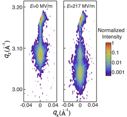
The structure of ferroelectric materials changes in applied electric fields through an effect known as piezoelectricity. For small electric fields piezoelectricity produces small strains that stretch the material but which are often not large enough to force the crystal to adopt a completely difrerent structure. We have found that by applying electric-field pulsese with very short durations we can produce strains that are very large, up to 2% in BiFeO3, a prototypical ferroelectric. This expansion is sufficient to show signs that the system is approaching a change in its structure. Large strains and large fields have the potential to yield a new mechanism to control the properties of electronic materials.
P. Chen, R. J. Sichel-Tissot, J. Y. Jo, R. T. Smith, S.-H. Baek, W. Saenrang, C.-B. Eom, O. Sakata, E. M. Dufresne, and P. G. Evans, "Nonlinearity in the high-electric field piezoelectricity of epitaxial BiFeO3 on SrTiO3," Appl. Phys. Lett. 100, 062906 (2012). (local) (publisher)
This work was supported by the National Science Foundation through grant number DMR-1106050. Student travel for experiments at Japan's Spring-8 light source was supported by the NSF through grant number OISE-0844424. (link to NSF) (DMR award abstract) (OISE award abstract)
Domain Dynamics in Superlattices

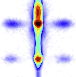
Superlattices consisting of stacks of alternating atomic-scale sheets of ferroelectric and dielectric materials have unusual properties because the of the constraints imposed by the thinness of the layers. These unusual properties include the creation of a domain struture consisting of stripes in which the polarization points in alternating up and down directions. These domains can be switched into a uniform polarization state but have unusual dynamics, including the potential to be switch very rapidly at high electric fields.
J. Y. Jo, P. Chen, R. J. Sichel, S. J. Callori, J. Sinsheimer, E. M. Dufresne, M. Dawber, and P. G. Evans, "Nanosecond Dynamics of Ferroelectric/Dielectric Superlattices," Phys. Rev. Lett. 107, 055501 (2011). (local) (publisher)
This work was supported by the Department of Energy, Office of Basic Energy Sciences through grant number DEFG02-10ER46147. (link)
New Probes for Photoinduced Charge Transfer

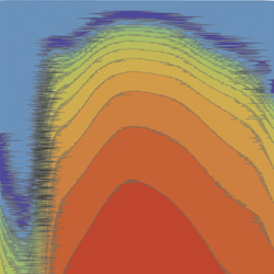
Interfaces have a crucial role in low-cost optoelectronic devices including solar photovoltaics and hybrid light emitting diods. These interfaces are formed between inorganic semicondcutor materials, often a semiconducting metal oxide such as ZnO, and organic semiconductors or dyes. In solar photovoltaics, light is absorbed in the semiconductor or dye and a charge is subsequently transferred to the semiconducting oxide. Better control of the structure and molecular conformations at the oxide surface will maximize the charge transfer rate, and increase electron lifetimes in the oxide before recombination occurs. We have developed new electrical tools based on field-effect transistor devices that will allow the transfer and recombination processes to be studied directly, including how these processes are modified by changing the chemical structure of the interface.
J. W. Spalenka, E. M. Mannebach, D. J. Bindl, M. S. Arnold, and P. G. Evans, "Spectral resolution of states relevant to photoinduced charge transfer in modified pentacene/ZnO field-effect transistors," Appl. Phys. Lett. 99, 193304 (2011). (local) (publisher)
J. W. Spalenka, P. Paoprasert, R. Franking, R. J. Hamers, P. Gopalan, and P. G. Evans, "Molecular control of pentacene/ZnO photoinduced charge transfer," Appl. Phys. Lett. 98, 103303 (2011). (local) (publisher)
This work was supported by the National Science Foundation through the University of Wisconsin Materials Research Science and Engineering Center through grant number DMR-1121288. (link)
Archived Research Nuggets
Archived Research Nuggets (link)