X-ray nanobeam diffraction experiments used tightly focused x-ray nanobeams to provide new ways to characterize the nanoscale structure of materials. These methods produce complicated distributions of scattered x-ray intensity that can be understood using optical simulations.
The programs on this web page simulate the diffraction pattern produced from an x-ray nanobeam diffraction experiment characterizing an epitaxial thin film or superlattice. These types of thin film materials are the key component of electronic and magnetic devices, optoelectronic materials for semiconductor lasers, and emerging functional materials such as ferroelectric and multiferroic nanomaterials
The calculation is based on the propagation of coherent, monochromatic beam through focusing optics to the sample. The scattering from the sample is computed in the kinematic approximation by computing its lattice sum, which can be used to compute the amplitude of the scattered x-ray wavefield using the product of the lattice sum and the incident beam at the sample. The distribution of x-ray intensity in the final diffraction pattern is computed using the square magnitude of the scattered amplitude.
Development of Nanobeam Diffraction Simulator
Kinematical Diffraction Simulator (August, 2016):
Eli Mueller and Jack Tilka
Dynamical Diffraction Simulator (April, 2019):
Karl Gardner
Simulation Methods
Experimental Setup
The simulation on this webpage matches the experimental arrangement for an experiment characterizing Si/SiGe heterostructures by Tilka et al. at Sector 26 of the Advanced Photon Source [1]. Crucially, the sample is placed at the center of rotation of a diffractometer and characterized using radiation at the first order focus of the zone plate.
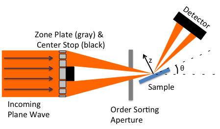
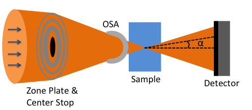
The parameters of the focusing optics and a diagram of the experiment are shown below.
Fig.1 Diagrams of the optical arrangement for the simulation, viewed (a) from above the scattering plane and (b) looking along the surface normal towards the sample.
Incident Beam
Photon energy: 10 keV
Fig. 1(b)
Zone Plate
Material: Gold
Diameter: 160 μm
Thickness: 400 nm
Outermost zone width: 30 nm
Focal length: 38.7 mm
Center Stop
Material: Gold
Diameter: 60 μm
Thickness: 70 μm
Order Sorting Aperture
Material: Platinum
Diameter: 30 μm
Distance from zone plate: 34.6 mm
Detector
Distance from sample: 1013 mm
Computational Methods
Incident Beam
The incident beam was simulated by propagating a radially symmetric wavefield of unity amplitude through the zone plate to the order sorting aperture (OSA) and from the OSA to the first order focus. The phase pattern introduced into the beam by the zone plate was calculated at each radial point and propagated to the OSA using the Fresnel diffraction integral operator [2]. The wavefield at points outside the aperture of the OSA was set to 0. The beam was propagated from the OSA to the first order focus using the same propagation method.
The Matlab code used to generate the incident beam is listed under source code and can be modified to simulate experiments using other optical arrangements, including different zone plate geometries, OSA diameters, and x-ray photon energies.
The simulation as implemented here is based on the focused wavefield produced using the parameters listed in the table above. In practice, the wavefield at the sample was saved to a binary data file that the web simulation reads and uses to simulate the diffracted intensity distribution.
Lattice Sum Simulation
We have also included a simulation of an intermediate step in the simulation of the nanobeam diffraction experiment. The lattice sum simulation creates a plot of the square magnitude of the lattice sum computed from the sample over a range of reciprocal space coordinates, here converted to corresponding incident angles of an incident plane wave x-ray beam. A one dimensional lattice sum is calculated in this simulation. This plot represents the structural information of the sample along the axis of reciprocal space extending along the surface normal. The range and discretization of the plot is set by user input.
The lattice sum calculation for each incident angle is outlined below.
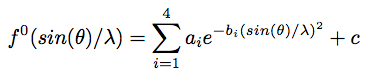
The scattering factor for the elemental constituents of the sample is calculated. The scattering factor is computed from the 9 parameter equation using the Cromer-Mann coefficients and the following formula [3]:
The simulation here neglects the anomalous scattering and absorption contributions to the scattering factor.
Calculate the reciprocal space lattice positions of each wave vector for each layer of material. Because this simulation only considers structural information along one direction, the h and k positions are fixed at 0 and l changes with angle of incidence. The reciprocal space positions are used to calculate the unit cell structure factor at each layer.
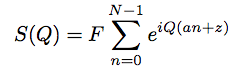
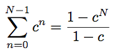
Add the lattice sums for each layer of material. The lattice sum for a single layer is given by the expression
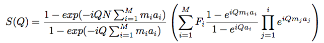
where a is the lattice constant, N is the thickness of the layer in number of unit cells, z is the depth of the bottom unit cell in the layer, and F is the unit cell structure factor. Q is the wave vector transfer, which is the difference between the incoming wave vector and the diffracted wave vector. For an arbitrary number of layers within a repeating superlattice, this expression is used to add the lattice sums for each individual layer in the sample. Using the geometrical series identity,
, the sum can be simplified to obtain the general expression below which is used in the simulation to calculate the lattice sum for any superlattice.
N is the number of superlattice layers, M is the number of separate layers of material within each repeating superlattice layer, mi is the thickness of the ith layer in the superlattice layer, ai is the lattice constant of the ith layer in the superlattice, Fi is the unit cell structure factor for the ith layer in the superlattice layer. In deriving this expression, the z = 0 point is set to be at the top of the sample.
Click 'derivation' to download the file that shows the derivation of the lattice sum expression used in the simulation.
Diffraction Pattern Simulation
The diffraction simulation reads the data file generated by the incident beam optical simulation described above. The data file represents the intensity of each wave vector, K, in the incident beam spectrum. The calculation of the diffraction pattern from the incident beam is outlined below.
Generate a set of wave vectors representing each component of the incident beam spectrum. The range and discretization of the wave vectors is arbitrarily set by the real space coordinates of the incident beam spectrum. The wave vectors are then rotated into the sample frame so that the z direction is perpendicular to the surface of the sample.
The z component of each wave vector in the sample frame is proportional to the wave vector transfer.
Calculate the reciprocal space lattice positions of each wave vector for each layer of material. Again, the h and k positions are fixed at 0 and l changes with angle of incidence of the wave vector. The unit cell structure factor is calculated using the reciprocal space lattice positions.
Calculate the lattice sum for each incident wave vector using the same method outlined in the lattice sum simulation. The diffraction pattern is then computed by taking the square magnitude of the product of the incident beam spectrum and the lattice sum.
Approximations/Assumptions
Elemental scattering factors are used in the simulation, i.e. ionic scattering factors are neglected
Angular beam divergence of 0.24 degrees is neglected in scattering factor calculation
Anomalous dispersion effects in the atomic scattering factor are neglected
Simulation is in the kinematical limit
X-ray absorption is neglected, simulation is only accurate for sample thicknesses much less than one attenuation length
OSA is perfectly opaque
Beam is perfectly monochromatic and coherent
Material Scattering Factor
For alloy materials, the atomic scattering factor is calculated, then a weighted average based on the composition of each material is used to calculate the material scattering factor. These averages are listed below.
SiGe - Scattering factor is calculated assuming 70% Silicon and 30% Germanium.
To download the source code for each part of the simulation, click the buttons below.
Incident Beam
Diffraction Simulation
Lattice Sum Simulation
References
J. A. Tilka, J. Park, Y. Ahn, A. Pateras, K. C. Sampson, D. E. Savage, J. R. Prance, C. B. Simmons, S. N. Coppersmith, M. A. Eriksson, M. G. Lagally, M. V. Holt, and P. G. Evans, J. Appl. Phys. 120, 015304 (2016)
A. Ying, B. Osting, I. C. Noyan, C. E. Murray, M. Holt, and J. Maser, J. Appl. Cryst. 43, 587 (2010)
Rupp, B., Calculation of atomic scattering factors, August 31, 2016, http://www.ruppweb.org/Xray/comp/scatfac.htm
Acknowledgments
Eli Mueller acknowledges support from the U. S. National Science Foundation for the development of the web-based simulation through contract number DMR-1609545. Jack Tilka acknowledges support from the Department of Energy Office of Basic Energy Sciences through contract number DE-FG02-04ER46147 for the development of the simulation methods.
 X-Ray Nanobeam Kinematical Diffraction Simulator